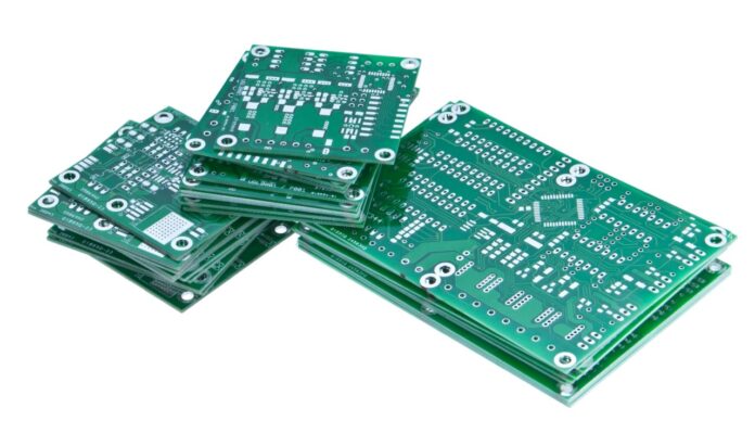
In recent years, PCB manufacturing in India has reached a value of US$ 2.75 Billion in 2020 and is expected to grow at 18% CAGR. It will reach US$ 7.45 billion by the year 2026.
India is becoming a major consumer electronic market in the Asia Pacific region. From computers, tablets, cell phones, and other electronic gadgets are sold highest in India than in any other country. To meet the demand there are numerous PCB manufacturers in different regions of India. And this demand in consumer electronics boosts the Indian PCB manufacturing market.
Most people don’t know the full form of PCB and what are the manufacturing stages? It is a Printed Circuit Board. In this article, we will discuss the various composition of PCB, assembly, and design processes.
First, let’s see What is PCB?
PCB is referred to as Printing Circuit Boards. Sometimes it is also known as printed wiring boards or printed wiring cards. Before the invention of PCB, the process is done by point-to-point wiring. Due to this short circuits are frequent as the wire insulation started to crack and age.
PCB Properties
PCB is an electric circuit that is used for linking electronic and electrical components without wires. It is used to connect surface-mounted and socket components in different applications. The copper-laminated boards where components are mounted are made from fiberglass, epoxy composites, or other various composite materials. These PCBs start from a single layer to multiple layers. PCBs are used in various applications such as computers, cell phones, television sets, laptops, LED lighting, and other gadgets.
The PCB is divided into Bare PCBs and Populated PCBs based on manufacturing.
Different Types of PCBs
- Single and Double-layer Rigid PCB
- Multiplayer
- Flexible
- Rigid-Flex
- Metal Core
Different types of Laminates used in PCB
- FR-4
- CEM-1
- Paper
- Others
PCB Composition
FR4
The base material used for PCB is fiberglass commonly known as FR4. It gives it rigidity and thickness. There are also some PCBs built on flexible high-temperature plastics like Kapton or others. The general PCBs are a thickness of 1.6 mm. But the cheaper PCBs are made of epoxies or phenolics and have no durability like FR4.
Copper
The next layer of the PCB is Copper foil. The copper is laminated on board with heat and adhesive. For the double-sided PCBs, copper is applied on both sides. For the lower price gadgets, the copper is applied only single side of the PCB. The copper thickness is depending on the weight, the majority of PCBs have 1 ounce of copper per square foot. Sometimes it is 2 or 3 once copper for high power applications.
Soldermask
The top layer on copper foil is known as a solder mask. The solder mask layer gives the PCB its unique color. It provides insulation to the copper traces from contact from metal, solder, or other conductive bits. Soldermask is commonly in green color but it can be any color.
Silkscreen
This silkscreen layer is applied on top of the solder mask layer. The silkscreen displays the letters, numbers, or symbols on PCB. This will help to understand the board. The silkscreen labels are used to show the function of a pin or LED on PCB.
Generally, the silkscreen is white. It is available in multiple colors like black, grey, red, or yellow. However, there is only single color on a single board.
Indian PCB Market Analysis
The PCB manufacturing in India is in full gear. The primary reason is a boom in the consumer electronic sector which stays high for at least the upcoming few years. This is due to urbanization, improved living standards, and increased income of individuals. The PCBs are an integral part of these devices. and for this Indian Government has encouraged PCB manufacturers to meet the demand by initiatives such as Made in India, Digital India, and National Policy on Electronics. The local pcb manufacturer provide the PCBs to domestic electronic goods manufacturers. Now with the advanced PCB technology and designing PCB manufacturers can minimize the size of PCB which helps to reduce the size of a product without compromising the performance.


